Project / 01
KeyTag PCB
- Hardware
- PCB design
- Firmware
- RF
A rechargeable Bluetooth keychain tracker that reports through Apple's Find My network — and a first from-scratch four-layer board.
Snapshot
The fast read
- Role
- Design, layout, assembly
- Year
- 2026
- Status
- In progress
- Type
- Personal
- Team
- Solo
- Stack
- KiCad, ESP32-C3-MINI-1, TP4056, MAX17048, NTAG213, SSD1306, JLCPCB 4-layer
- Tags
- Hardware · PCB design · Firmware · RF
Section
Why build it
I wanted to learn circuit and PCB design properly, and I needed a real project rather than an exercise. I worked through Phil's Lab's KiCad tutorial and built the tutorial board first, which taught me the tool. Then I wanted something I would actually carry.
A keychain tracker packs most of what I wanted to practise into something small: power and battery management, with USB-C charging, load sharing so it runs from USB while charging, a 3.3 V rail and a fuel gauge measuring the cell directly; RF, with a 2.4 GHz Bluetooth module at one end and a 13.56 MHz NFC antenna I drew myself as copper on the board; layout discipline, with real return-path decisions, decoupling placement, keepouts and a fab house's rules to meet; firmware bring-up, getting the board onto Apple's Find My network; and hand assembly and debugging with nothing but a multimeter and a soldering iron.
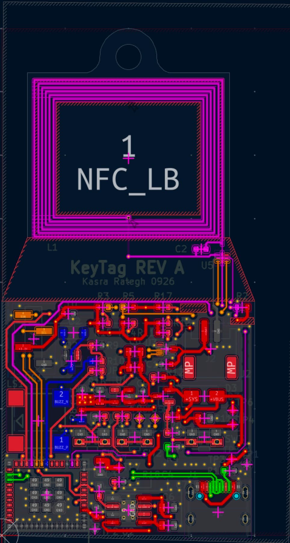
Squeezing all of that into a keychain is what made it hard. The NFC antenna cannot have a ground plane under it, so almost half the board has no ground plane at all. That one constraint shaped the entire layout.
Section
The board
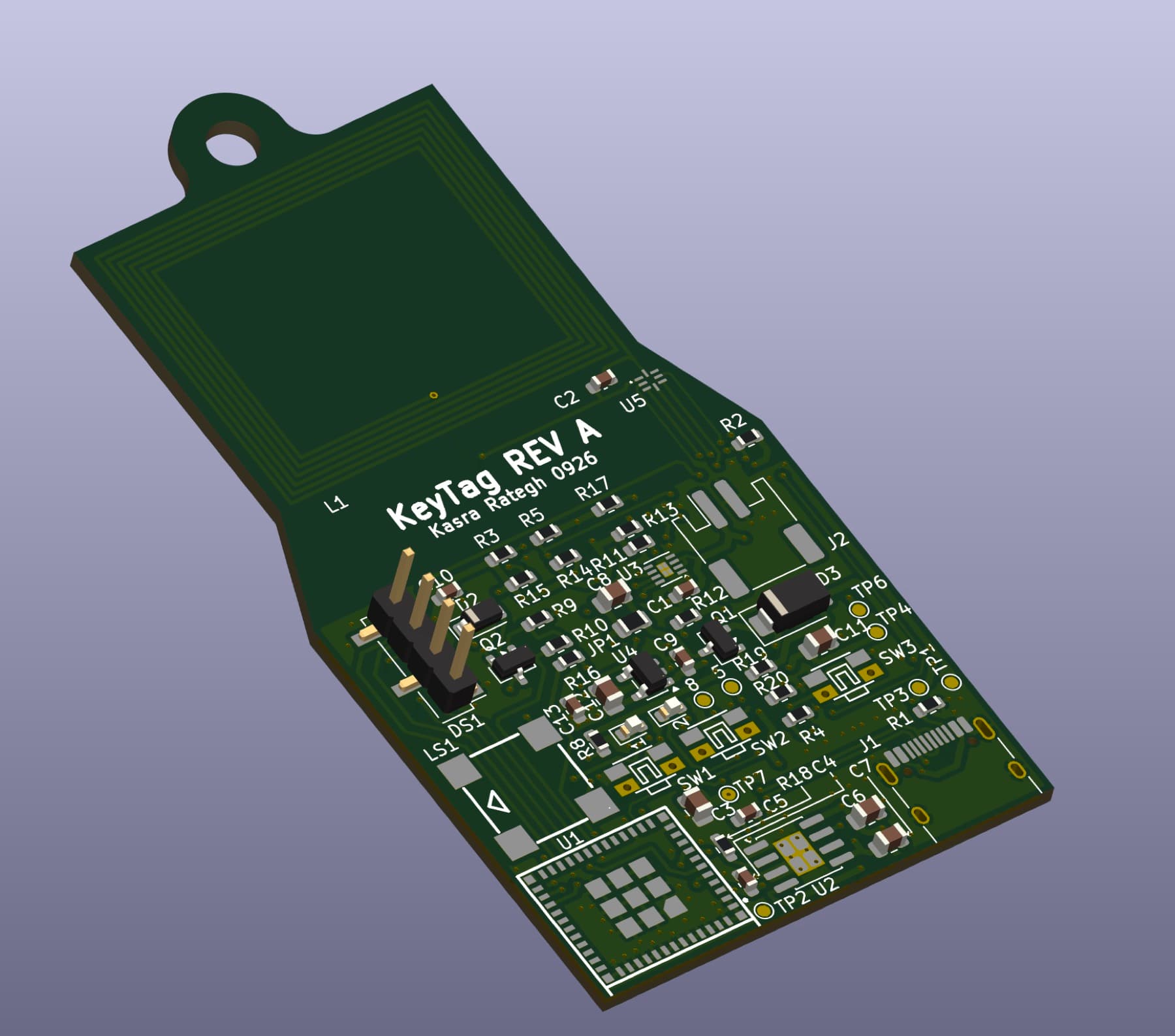
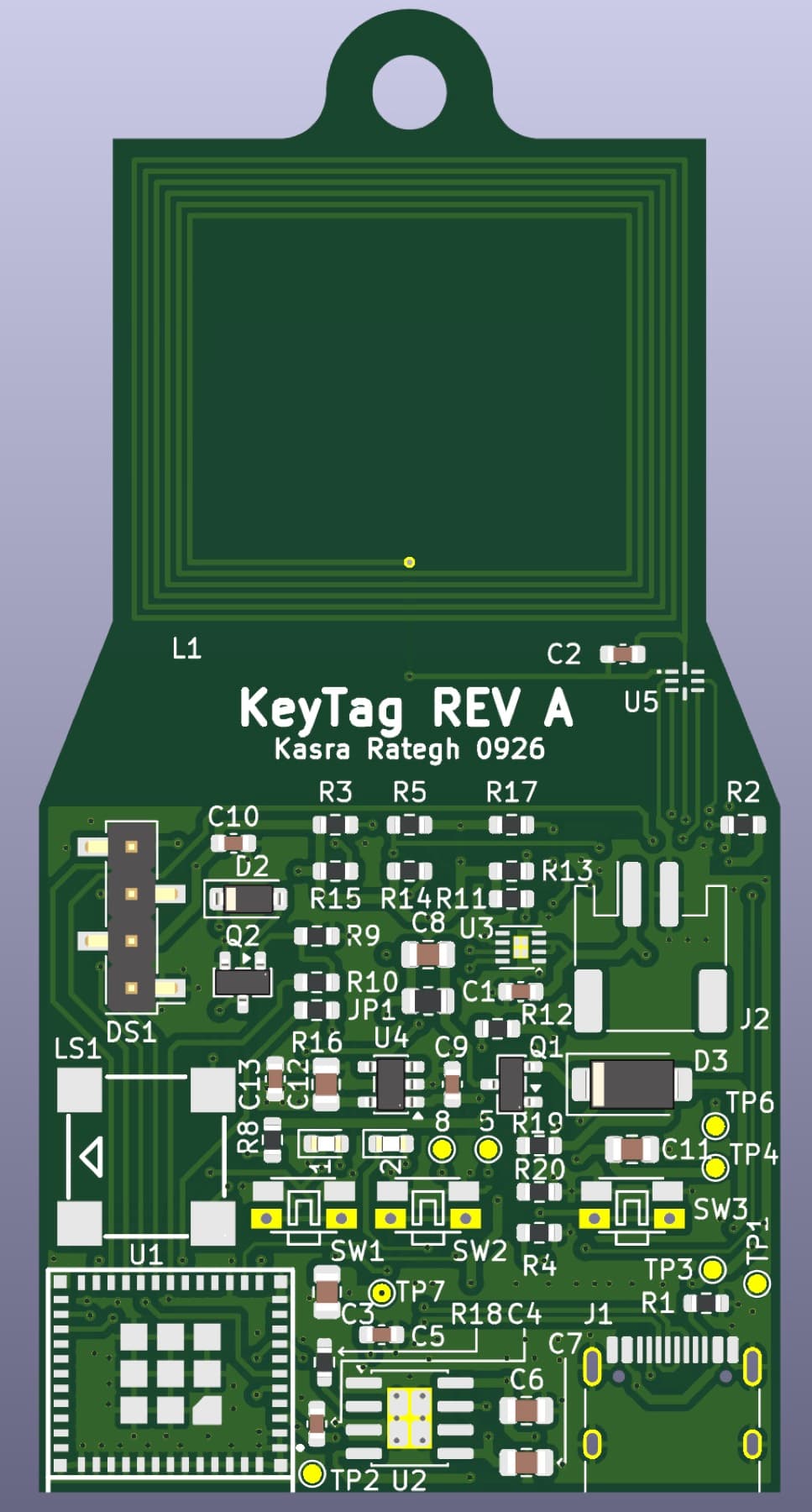
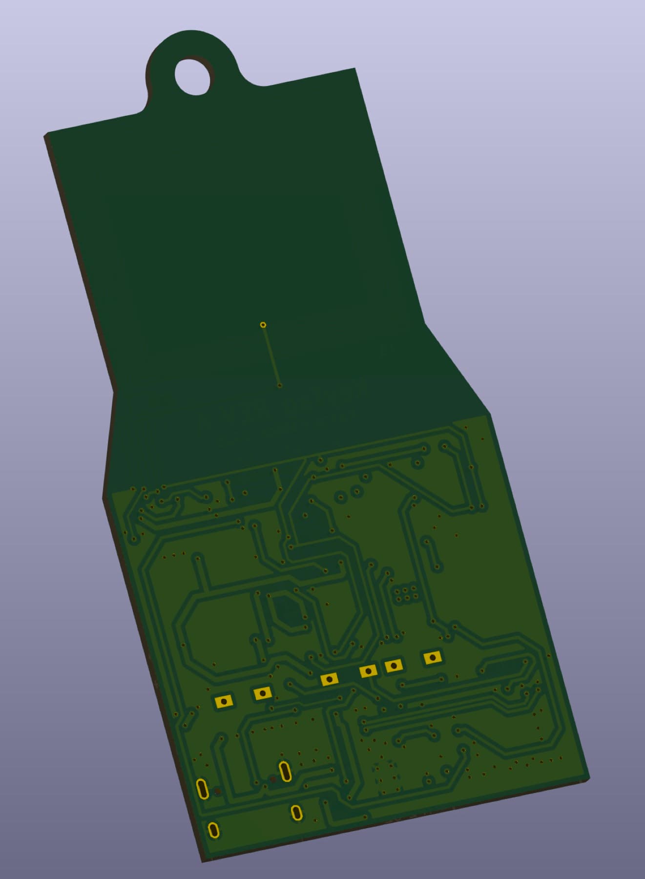
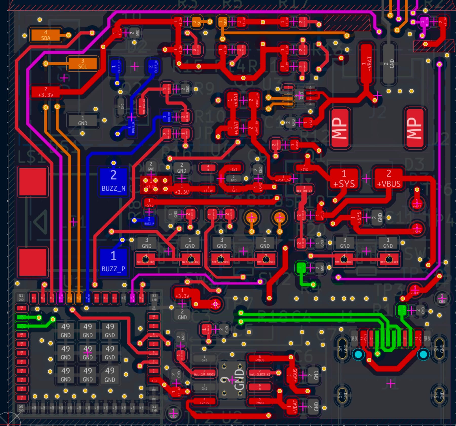
A 40 × 80 mm four-layer board, 1.6 mm thick on JLCPCB's JLC04161H-3313A stackup, narrowing to 32 mm at the tapered NFC head. A LiPo pouch cell sits on the back; three buttons and a USB-C port sit on the front, along with every component — the back carries only the battery.
An ESP32-C3-MINI-1 module does the work, with Bluetooth and its own edge antenna, programmed over native USB so there is no separate programming header. USB-C feeds a TP4056 charger; a P-MOSFET load-share path and an LDO produce the 3.3 V rail, so the tag runs from USB while the cell charges. A MAX17048 fuel gauge sits right at the battery connector over I²C, measuring the cell itself rather than the rail.
For output there is an SSD1306 OLED, a buzzer and two LEDs. An NTAG213 gives it a tag you can touch a phone to, driven by the trace antenna in the head. Find My reporting goes through the OpenHaystack approach.
Section
Engineering decisions
Four layers instead of two, for return paths rather than routing room. Running signals over a ground plane came out about twice as good on inductance: 0.390 against 0.774 nH/mm.
Hand assembly instead of JLCPCB's. Assembly was the original plan and it would have been more reliable, but the point of the project is to learn, so I ordered bare boards and parts and will solder them myself.
An e-ink display was cut for Rev A. The OLED stayed, mostly for personality. The USB ESD clamp and its 0 Ω links came out too, so the data lines now run straight from the connector to the module, and the test points went from twelve to eight.
Two things I rejected. A clipped-lead header under the battery, because its safety depended on tape holding. And rotating the NFC chip 180°, which sounds like it should help and does not: both signals approach its two landlocked middle pads from the same side, so no rotation fixes it.
The Bluetooth antenna is the module's own; the NFC antenna is a loop I drew in copper rather than a bought coil.
Section
Checking my own work
With no scope and no bench supply, the only way to trust the board before it exists is to check the design files. I wrote six Python checkers that read the KiCad files directly — board setup, placement, documentation against the board, schematic spec, clearance, and a corner model.
They earned their keep by failing. Opening a file standalone once wiped the entire board setup: minimum clearance dropped to zero, and DRC cheerfully reported no errors against the wiped rules. I recovered from KiCad's auto-backup and wrote a guard script so it cannot happen quietly again.
Renaming designators silently disabled a test-point checker: four checks kept passing while checking nothing. The clearance checker had its rotation sign backwards and invented shorts on exactly the five parts rotated by ±90°. Getting the placement order wrong left the test points with whatever board space was left over. Asking a simple question — is the buzzer under the screen? — exposed that the OLED module was not drawn in the board file at all. The stackup did not add up to 1.6 mm at one point. And figures written down early and never re-checked went stale, causing about eleven errors downstream.
Section
Schematic
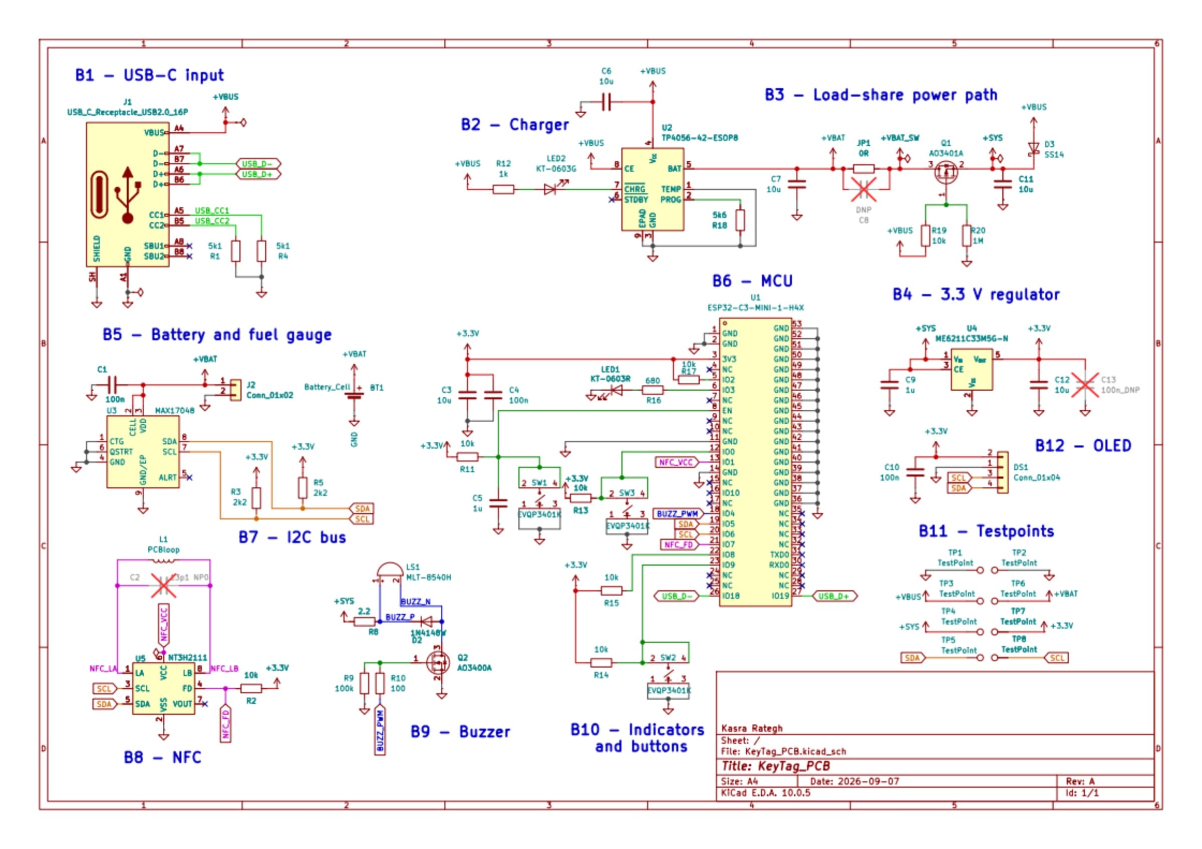
One page, blocked by function: USB-C input, charger, load-share path, 3.3 V regulator, battery and fuel gauge, MCU, I²C bus, NFC, buzzer, indicators and buttons, test points, and the OLED header. The full-size PDF and the bill of materials are linked below.
| Ref | Part | Does what |
|---|---|---|
| U1 | ESP32-C3-MINI-1-H4X | MCU and Bluetooth, with its own edge antenna |
| U2 | TP4056-42-ESOP8 | Single-cell LiPo charger from USB-C |
| U3 | MAX17048 | Fuel gauge on I²C, at the cell |
| U4 | ME6211C33M5G-N | 3.3 V LDO |
| U5 | NT3H2111 | NFC tag |
| Q1 | AO3401A | P-MOSFET, load-share path |
| Q2 | AO3400A | N-MOSFET, buzzer drive |
| D3 | SS14 | Schottky on the system rail |
| L1 | PCB loop | NFC antenna, 6 turns, 30 × 25 mm |
| J1 | USB-C receptacle | Power in and native USB |
| J2 | JST PH | Battery connector |
| DS1 | 1×04 header | OLED |
| LS1 | MLT-8540H | Buzzer |
| SW1–SW3 | EVQP3401K | Buttons |
| LED1, LED2 | 0603 | Status indicators |
| TP1–TP8 | Test pads | The whole instrumentation plan |
Section
Where it stands
The design is finished: schematic, placement, routing and pours. The board carries 59 footprints, 602 tracks and 191 vias, with no unrouted connections and clearance checks passing.
Five bare boards are ordered from JLCPCB, with the parts coming separately from LCSC. Next is hand assembly, then bring-up — power first, measured at the test points with a multimeter, then firmware.
Instrumentation is deliberately thin: eight test points and the fuel gauge are the entire plan, and none of them may hide under the display. There is no deadline on this one, on purpose.
Links
Elsewhere
Next project